
CBSE Class 12 Physics Chapter 14 Semiconductor Electronics Multiple Choice Questions And Answers
Question 1. Vm is the maximum voltage between the ends of the secondary terminal of a transformer used in a half-wave rectifier. When the PN junction diode is reverse-biased, what will be the potential difference between the two ends of the diode?
- Zero
- \(\frac{V_m}{\sqrt{2}}\)
- Vm
- 2 Vm
Answer: 2. \(\frac{V_m}{\sqrt{2}}\)
Read and Learn More Important Questions for Class 12 Physics with Answers
Question 2. The band gaps of an insulator, semiconductor, and conductor arc respectively Eg1, Eg2, and Eg3 The relationship between them can be given as _______.
- Eg1 = Eg2 = Eg3
- Eg1 < Eg2 < Eg3
- Eg1 > Eg2 > Eg3
- Eg1 < Eg2 > Eg3
Answer: 3. Eg1 > Eg2 > Eg3
Question 3. A potential barrier of 0.2V exists across a pn junction. If the depletion region is 5.0 x 10⁻⁷ m wide, then the intensity of the electric field in this region is ___ V/m
- 1 x 10⁵
- 4 x 10⁵
- 1 x 10⁶
- 2 x 10⁵
Answer: 2. 4 x 10⁵
Question 4. When will the conductivity of a Ge semiconductor decrease?
- On adding acceptor impurity
- On adding donor impurity
- On making UV light incident
- On decreasing the temperature
Answer: 4. On decreasing the temperature
Question 5. In an n-type semiconductor, which of the following statements is true:
- Electrons are the majority carriers and tri-valent atoms are the dopants.
- Electrons are the majority carriers and pentavalent atoms are the dopants.
- Holes are minority carriers and pentavalent atoms are the dopants.
- Holes are majority carriers and tri-valent atoms arc the dopants.
Answer: 2. Electrons arc majority carriers and pentavalent atoms are the dopants.
Question 6. When a forward bias is applied to a p-n junction, it
- Raises the potential barrier
- Reduces the majority carrier current to zero
- Lowers the potential barrier
- None of the above
Answer: 3. Lowers the potential barrier
Question 7. In half-wave rectification, what is the output frequency if the input frequency is 50 Hz?
- 0
- 100 Hz
- 50 Hz
- 25 Hz
Answer: 3. 50 Hz
Question 8. _______ as an impurity, when added in Si or Gc P-type semiconductor is obtained.
- Antimony
- Arsenic
- Phosphorus
- Boron
Answer: 4. Boron
Question 9. In an intrinsic semiconductor, the density of free electrons is nc and the number density of holes is nh then ________.
- nc >> nh
- nc = 2nh
- nc = nh
- nc << nh
Answer: 3. nc = nh
Question 10. In an unbiased p-n junction, holes diffuse from the p-region to the n-region because,
- Free electrons in the n-region attract them
- They move across the junction by the potential difference
- Hole concentration in the p-region is higher as compared to the n-region
- All the above
Answer: 3. Hole concentration in the p-region is higher as compared to the n-region
CBSE Class 12 Physics Chapter 14 Semiconductor Electronics Short Questions And Answers
Question 1.
- How does the energy gap of an intrinsic semiconductor change when doped with a trivalent impurity?
- In a p-n junction under equilibrium, there is no net current. Why?
Answer:
- Then some allowed energy levels are produced, situated in the energy gap slightly above the valence band, this arc is called acceptor energy levels. Due to this energy band gap decreases.
- Net current (diffusion and drift current) is zero for both electrons and holes because the diffusion current is equal and opposite to the drift current for both carriers.
Question 2. Explain the formation of the barrier potential in a p-n junction.
Answer:
The loss of electrons from the n-region and the gain of electrons by the p-region causes a difference in potential across the junction of the two regions.
- The polarity of this potential is such as to oppose the further flow of earners so that a condition of equilibrium exists.
- The p-n junction at equilibrium and the potential across the junction. The n-material has lost electrons, and the p-material has acquired electrons. The n-material is thus positive relative to the p-material.
Since this potential tends to prevent the movement of electrons from the n region into the p region, it is often called a barrier potential.
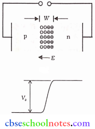
Question 3.
- Draw the circuit diagram of an illuminated photodiode and its I-V characteristics.
- How can a photodiode be used to measure the light intensity?
Answer:
2. The photocuring is directly proportional to the intensity of light this can be used for measuring the intensity of incident light.
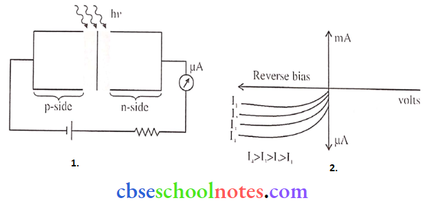
Question 4.
1. In the following diagram, is the junction diode forward-biased or reverse-biased?
2. Name two important processes that occur during the formation of a pn junction.
Answer:
1. Reverse biased as the p-side is connected to the lower potential and the n-side to the higher potential.
Two important phenomena occur during the formation of the pn junction:
2. (1) Diffusion: Due to the concentration gradient the majority of charge carriers from the p side (holes) and the majority of charge carriers (electrons) on the n side start diffusing towards their opposite side.
(2) Drift: As electron-hole pairs neutralize near the junction they leave behind immobile ions, these ions create an electric field from the n side to the p side due to which the minority charge carrier starts moving (drifting).
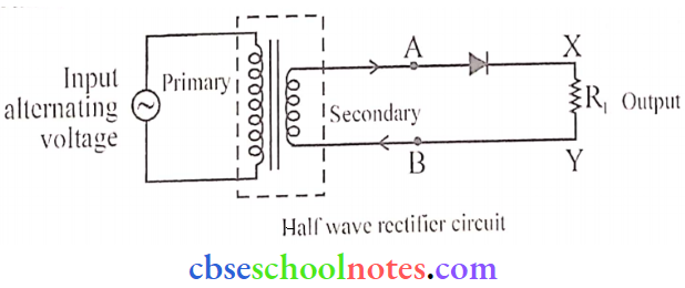
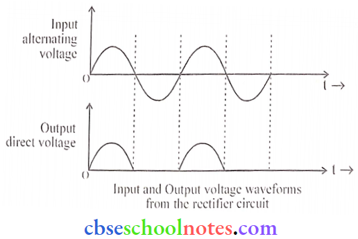
Question 5. Draw the circuit diagram of a half-wave rectifier and explain its working.
Answer:
Working of half wave rectifier: The secondary coil of a transformer supplies the desired alternating voltage across terminals A and B. When the voltage at A is in a positive cycle, the diode is in forward bias and it conducts current.
When A is at a negative cycle, the diode is in reverse bias and it does not conduct current only in the positive half-cycle of alternative current (ac), there is a current through the load resistor RL, and we gel output voltage.
Thus, We get a half-wave rectified output. So this circuit is called a half-wave rectifier.
Circuit Diagram:
Graphy:
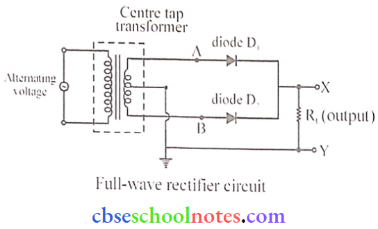
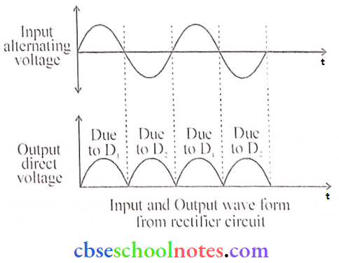
Question 6. Draw the circuit diagram of a full wave rectifier along with the input and output waveforms. Briefly explain how the output voltage/current is unidirectional.
Answer:
Working: When the positive half cycle of input a.c. signal flows through the primary coil, induced emf is set up in the secondary coil due to mutual induction. The direction of induced emf is such that the upper end of the secondary coil becomes positive while the lower end becomes negative.
- Thus, diode D1 is forward biased and diode D2 is reverse biased, so the current due to diode D1 flows through the circuit. The output voltage which varies per the input half cycle is obtained across the load resistance (RL).
- During the negative half cycle of input a.c. signal, diode D1 is reverse biased and diode D2 is forward biased. The current due to diode D2 flows through the circuit. The output voltage is obtained across the load resistance (RL ). The input and corresponding output voltage are predicted.
Since both the halves of input a.c. (wave) arc rectified, so the junction diode is called a full wave rectifier.
Circuit Diagram:
Graph:
Question 7. Distinguish between a conductor and a semi-conductor based on the energy band diagram.
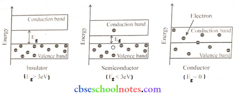
[Eg = Forbidden Energy gap]
Question 8. Show on a plot, the variation of resistivity of
- A conductor, and
- A typical semiconductor as a function of temperature.
Using the expression for the resistivity in terms of number density and relaxation time between the collisions, explain how resistivity in the case of a conductor increases while it decreases in a semiconductor, with the rise of temperature.
Answer:
Variation of resistivity With Temperature
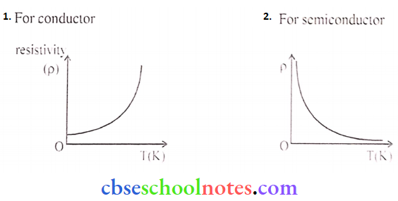
The resistivity of a material is given by
∴ \(\rho=\frac{m}{n e^2 \tau}\)
n ⇒ Number density
τ ⇒ Relaxation time
On increasing the temperature of the conductor relaxation time decreases while the number density remains constant. Due to this resistivity of the conductor increases.
In the case of semiconductors, on increasing the temperature relaxation time decreases but the number density increases. An increase in the number density is more effective than a decrease in the relaxation time. That’s why the resistivity of semiconductors decreases.
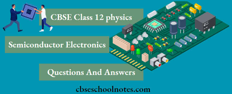
Question 9. Explain with the help of a diagram the formation of depletion region and barrier potential in a p-n junction.
Answer:
It is clear that the N-type semiconductor has a P-TYPC excess of free electrons and the P-type has an excess of holes therefore joined through a special process, electrons migrate towards the P-side and holes migrate towards the N-side due to concentration gradient.
The departure of an electron from the N-side to the P-side leaves a positive donor ion on the N-side and likewise hole leaves a negative acceptor ion on the P-side resulting in the formation of a depletion layer having widths 10-7m.
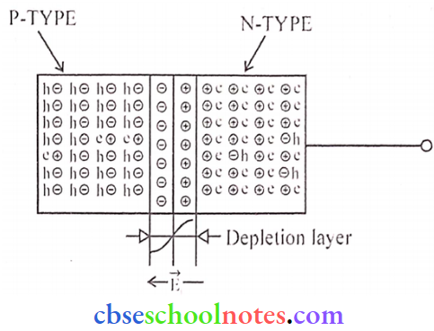
Depletion layer: It is the layer near the junction in which electrons arc absent on the n side and holes are absent on the p side.
Potential barrier: Due to the accumulation of immobile ions near the junction an electric potential difference (Vb) develops between the n side and the p side which acts as a barrier for further diffusion of electrons and holes.
Vb = Ei x d (volt)
Question 10. Draw the energy band diagrams for conductors, semiconductors, and insulators. Which band determines the electrical conductivity of a solid? How is the electrical conductivity of a semiconductor affected by the rise in its temperature? Explain.
Answer:
Energy Band Diagram:
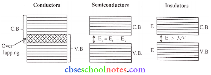
The conduction band determines the electrical conductivity of the solid.
On increasing the temperature of semiconductor electrical conductivity increases. When we increase the temperature, some of the covalent bonds get broken and e-hole pairs are generated.
CBSE Class 12 Physics Chapter 14 Semiconductor Electronics Long Questions And Answers
Question 1. Consider a thin p-type silicon (p-Si) semiconductor wafer. By adding precisely a small quantity of pentavalent impurity, part of the p-Si wafer can be converted into n-Si. There are several processes by which a semiconductor can be formed.
The wafer now contains p-region and nregion and a metallurgical junction between p-, and n- region. Two important processes occur during the formation of a p-n junction: diffusion and drift.
We know that in an n-type semiconductor, the concentration of electrons (number of electrons per unit volume) is more compared to the concentration of holes. Similarly, in a p-type semiconductor, the concentration of holes is more than the concentration of electrons.
During the formation of the p-n junction, and due to the concentration gradient across p-, and n- sides, holes diffuse from p- side to n-sidc (p → n) and electrons diffuse from n-sidc to p-sidc (n → p). This motion of charge carriers gives rise to diffusion current across the junction.
(1). How can a p-type semiconductor be converted into an n-type semiconductor?
- Adding pentavalent impurity
- Adding trivalent impurity
- Not possible
- Heavy doping
Answer: 1. Adding pentavalent impurity
(2). Which of the following is true about n-type semiconductors?
- The concentration of electrons is less than that of holes.
- The concentration of electrons is more than that of holes.
- The concentration of electrons is equal to that of holes.
- None of the above.
Answer: 2. Concentration of electrons is more than that of holes.
(3). Which of the following is the reason for diffusion current?
- Diffusion of holes from p to n
- Diffusion of electrons from n to p
- Both (1) and (2)
- None of these
Answer: 3. Both (1) and (2)
(4). What are the processes that occur during the formation of a p-n junction?
- Drift
- Diffusion
- Both (1) and (2)
- None of these
Answer: 3. Both (1) and (2)